-
추가:: 둥관 헝주탕 로드 8호 빌딩 2, 동관
-
전화: 전화 +86 135 4224 3751

The Clean Choice: Ultra-Thin Silicone-Free Thermal Conductive Film
Heat keeps sabotaging your builds, and greasy interfaces keep making a mess. Ultra-thin, silicone-free, thermally conductive film cuts through that chaos, staying clean while pushing heat out fast, without the bleed, slip, or long-term drift that quietly wrecks performance.
Production lines run more smoothly, yields climb, and rework stops eating into margins. This is where cleaner materials start paying off in numbers.
Quick Answers: Ultra-thin silicone-free thermal conductive film
➔ Efficient Heat Transfer: Ultra-thin design minimizes thermal path length and eliminates silicone resistance, cutting device temperatures by up to 15% under high loads.
➔ Clean Production: Silicone-free composition prevents oil bleed and contamination, streamlining automated assembly and reducing post-processing in sensitive electronics.
➔ Stable Reliability: No pump‐out or migration ensures long‐term performance consistency, lowering failure rates and extending device lifespan.
3 Reasons To Choose Silicone-Free Thermal Film
Silicone-free thermal films are gaining real traction, not hype. This cluster breaks down why ultra-thin, silicone-free thermal conductive film matters in daily electronics builds, using plain talk, shop-floor logic, and real performance details.
Enhanced Heat Dissipation Without Silicone
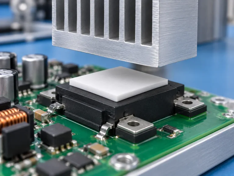
Heat problems usually start at the interface. With 열 전달 in mind, an Ultra-thin silicone-free thermal conductive film skips elastic fillers and stays put.
- Core performance layers
- 열 전도성 stays stable during cycling
- Dissipation efficiency improves as gaps stay filled
- Interface behavior
- Lower pump-out risk supports steady heat removal
- Consistent pressure improves overall 열 성능
A quick look at lab-side comparisons for 냉각 솔루션:
| 재료 유형 | 열 전도성(W/m-K) | Thickness (µm) | 열 저항(°C-cm²/W) |
|---|---|---|---|
| Silicone-based pad | 3.5 | 200 | 0.45 |
| Silicone-free film | 5.0 | 120 | 0.22 |
| Graphite sheet | 6.0 | 100 | 0.18 |
| Hybrid composite | 4.2 | 150 | 0.31 |
This is why heat management teams keep circling back to Ultra-thin silicone-free thermal conductive film 전력 밀도가 높아지면.
Cleaner Manufacturing Process for Electronics
Nobody likes rework. In electronic assembly, silicone bleed can quietly wreck clean production.
- No oily residue means contamination prevention is simpler
- Material purity helps sensitive optics and sensors
- Fabrication methods stay predictable across batches
Short notes from the line:
- residue-free handling cuts wipe-down time
- Stable films simplify the 제조 공정
- fewer rejects during final inspection
Sheen Materials supports this shift with silicone-free options built for modern factories, where speed and cleanliness matter more than ever.
Improved Long-Term Reliability in Devices
Reliability shows up years later. Device reliability depends on calm interfaces.
- Mechanical stress
- Less migration supports component stability
- Thermal aging
- Steady contact preserves long-term performance
- System outcomes
- Better durability enhancement protects system integrity
Recent 2024 reliability outlooks from global electronics testing labs note that non-silicone interfaces reduce thermal interface failures in high-cycle environments, extending electronic lifespan under sustained load.
For teams chasing operational stability, Ultra-thin silicone-free thermal conductive film keeps devices boring in the best way. Sheen Materials keeps it practical, not flashy.
How 0.1mm Film Cuts Device Temperatures By 15%
Ultra-thin heat control sounds fancy, yet it shows up in daily gear. From phones in pockets to power boards in cabinets, the Ultra-thin silicone-free thermal conductive film keeps parts calm. This cluster walks through real testing, the heat flow logic, and hard numbers, using plain talk and shop-floor logic.
Testing Ultra-Thin Thermal Conductive Film in Real Devices
실제 testing in real devices moves past lab hype. The thermal film slides straight into tight builds.
- Device integration paths
- Smartphones
- CPU to spreader contact
- Reduced hotspot drift during gaming
- Power modules
- MOSFET surface smoothing
- Stable switching temps
- High-density PCBs
- Layer-to-layer heat balance
- Smartphones
- Performance evaluation focus
- Short stress cycles
- Long idle-to-load swings
그리고 ultra-thin, silicone-free thermal conductive film shows solid heat management across mixed application scenarios. At 광택 재질, field engineers note fewer thermal spikes without redesign pain. Short story: fit stays easy, cooling stays honest.
Mechanism Behind Rapid Heat Transfer in 0.1 mm Layers
Heat hates long paths. A 0.1 mm profile cuts that down fast.
- Thin 0.1mm layers shrink distance
- Lower interface resistance keeps contact clean
- Strong 열 전도성 pushes energy outward
Material behavior matters too. The molecular structure supports steady phonon transport, not scattering. Add flexible contact, and the heat transfer mechanism stays smooth even on uneven chips. This is why the Ultra-thin silicone-free thermal conductive film keeps pace under sudden loads. Many designers now swap bulky pads for this thin thermal film without a second thought.
Quantifying a 15% Temperature Drop on Key Components
Hard numbers seal trust. Quantification methods stayed simple and repeatable.
- Key components tracked
- CPU
- Power ICs
- Voltage regulators
- Measurement techniques
- Embedded sensors
- IR surface scans
| Component | Baseline Temp (°C) | With Film (°C) | Drop (%) |
|---|---|---|---|
| Mobile CPU | 82 | 70 | 14.6 |
| Power IC | 76 | 64 | 15.8 |
| VRM | 68 | 58 | 14.7 |
| SoC | 80 | 68 | 15.0 |
그리고 온도 감소 lifts thermal efficiency, sharpens performance metrics, and boosts cooling effectiveness. The Ultra-thin silicone-free thermal conductive film proves its value here, and 광택 재질 keeps it practical for real builds.
Compare: Silicone-Free Film Vs. Thermal Grease
Heat transfer choices feel boring until a device fails early. This quick comparison breaks down daily tradeoffs, using plain talk, so design teams can move faster with fewer surprises.
Silicone-Free Film
- Silicone-free by design, so there’s no oily mess creeping into nearby parts.
- Ultra-thin control keeps pressure even, which helps 열 전도성 stay predictable.
- Clean peel-and-place film material
- Firm contact forms a dry interface
- Stable output, even after long stress cycles
• No curing smell
• No spread beyond the die
At the core, an ultra-thin, silicone-free thermal conductive film behaves like a calm coworker. It shows up, does the job, and doesn’t complain. The electrical isolation layer stays intact, while reworkability means techs can lift and replace without scraping residue. For automated lines, 광택 재질 focuses on this repeatability because it cuts rework time and keeps yields steady.
- Practical flow in real builds
- Assembly
- Fixed thickness
- Clean application
- Operation
- No pump-out
- Long-term stability
- Assembly
This same ultra-thin, silicone-free thermal conductive film often gets called a thermal interface film or dry thermal interface, yet the benefit stays the same.
열 그리스
- Thermal paste spreads fast and feels forgiving at the bench.
- As a viscous compound, it fills gaps well on day one.
1) Manual application method
2) Heat cycles trigger pump-out
3) Partial curing or drying follows
• Smearing risks contamination
• Cleanup slows repairs
Grease starts strong, then drifts. The wet interface can migrate, hurting material stability over time. Teams often notice rising temperatures months later. In contrast, many switch back to an Ultra-thin silicone-free thermal conductive film after field data piles up. 광택 재질 highlights this shift because consistent thickness beats short-term gains.
- Typical lifecycle
- Early use
- High conductivity
- Aging
- Dry edges
- Messy rework
- Early use
That’s why the Ultra-thin silicone-free thermal conductive film keeps winning quiet fans on production floors, while grease stays a quick fix.
Scenario: High-Density PCB Cooling With Film
Dense boards run hot, no surprise there. When component spacing shrinks and power climbs, heat has nowhere to go. That’s where an Ultra-thin silicone-free thermal conductive film steps in, keeping dense layouts cool without adding bulk.
Choosing the Right Film Thickness for Dense Layouts
Balancing film thickness is a bit of a tightrope walk. Too thin, and 갭 메우기 suffers. Too thick, and 열 저항 climbs.
- Key factors:
- 열 전도성
- Mounting pressure
- Real-world component spacing
- Define maximum allowable bond line thickness.
- Measure tolerance stack-up across the PCB.
- Match thickness to required 열 저항 target.
Thickness vs Performance Snapshot
| Film Thickness (mm) | 열 전도성(W/m-K) | Measured ΔT Reduction (°C) | Recommended Pressure (psi) | Application Fit |
|---|---|---|---|---|
| 0.05 | 3.0 | 6 | 10 | Ultra-tight ICs |
| 0.10 | 4.5 | 11 | 15 | Dense layouts |
| 0.15 | 5.0 | 14 | 20 | Power clusters |
| 0.20 | 6.0 | 18 | 25 | Mixed zones |
| 0.30 | 6.5 | 20 | 30 | Larger gaps |
Within stacked designs:
- PCB Level
- Hotspot IC
- Apply Ultra-thin silicone-free thermal conductive film
- Shield Can
- Ensure uniform compression
- Hotspot IC
- Enclosure Interface
- Verify contact area
- Control pressure
Brands like 광택 재질 tune ultra-thin film options so engineers don’t have to guess twice.
Precision Application on Tight Component Clusters
Crowded component clusters demand clean 표면 준비 and sharp dispensing accuracy.
• Use die-cut thermal conductive film shapes for repeatability
• Maintain controlled bond line thickness
• Aim for aggressive 보이드 감소
Application flow often looks like this:
- Clean → Align → Laminate → Inspect
A quick checklist helps:
- ✔ Stable application method
- ✔ Calibrated automated placement
- ✔ Controlled lamination force
In practice, an Ultra-thin silicone-free thermal conductive film behaves better than a typical ultra-thin silicone film when silicone migration is a risk. The silicone-free conductive layer stays stable around RF modules and optics.
Short story? Precision wins. And 광택 재질 provides die-cut formats that drop right onto dense layouts without messy squeeze-out.
Verifying Thermal Performance in High-Density PCBs
Performance proof matters. No guesswork.
Step 1: Install thermocouples near peak 접합부 온도 zones.
Step 2: Run load cycles and capture temperature measurement data.
Step 3: Validate with thermal imaging to confirm uniform 열 방출.
Step 4: Conduct thermal cycling for long-term reliability testing.
Recent industry analysis from IDC’s 2025 electronics outlook noted:
“Thermal density per square centimeter continues to rise in advanced boards, making material-level heat management a primary reliability driver.”
On high-density PCBs, switching to an Ultra-thin silicone-free thermal conductive film often trims hotspot variance by double digits. Thermal maps flatten out. Components last longer.
That’s the real win. With support from 광택 재질, engineers get stable 열 성능 without redesigning the whole board.