-
추가:: 둥관 헝주탕 로드 8호 빌딩 2, 동관
-
전화: 전화 +86 135 4224 3751

Solving Heat Issues Using Custom-Shaped Boron Nitride Pads
Writing block: Custom-shaped boron nitride pads step in when heat starts acting like a stubborn houseguest, pushing electronics to their limits and draining performance faster than expected.
Smart buyers cut the noise, choosing materials that cool efficiently, insulate safely, and fit tight designs without costly redesign headaches.
Key Highlights: Custom-shaped boron nitride pads
➔ Types & Materials – From hexagonal and pyrolytic BN to ceramic composites and advanced nitride ceramics, each offers tailored thermal conductivity, electrical insulation, and chemical stability.
➔ Core Benefits – High in‐plane heat spreading, dielectric strength for leakage prevention, and mechanical resilience against wear and oxidation ensure reliable performance.
➔ Targeted Uses – Ideal as thermal interface pads in power electronics, RF modules, LED assemblies, and compact semiconductor packaging.
Layered: Types Of Custom-Shaped Boron Nitride Pads
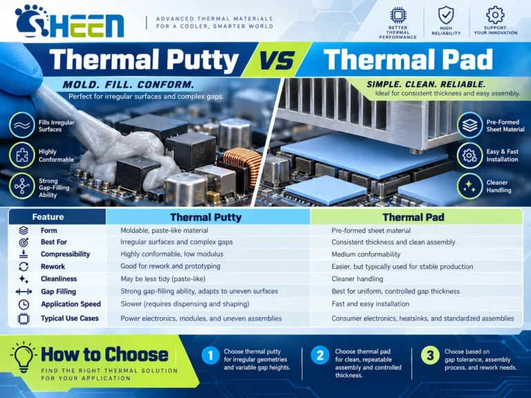
Custom-shaped boron nitride pads are not just flat sheets tossed into electronics. Break the phrase down—custom-shaped, boron nitride, pads—and you get the story: geometry tailored to fit, high-performance ceramic chemistry, and practical thermal pads that sit exactly where heat builds up. From boron nitride pads in power modules to shaped BN heat spreaders in RF systems, these solutions keep devices cool without adding electrical risk.
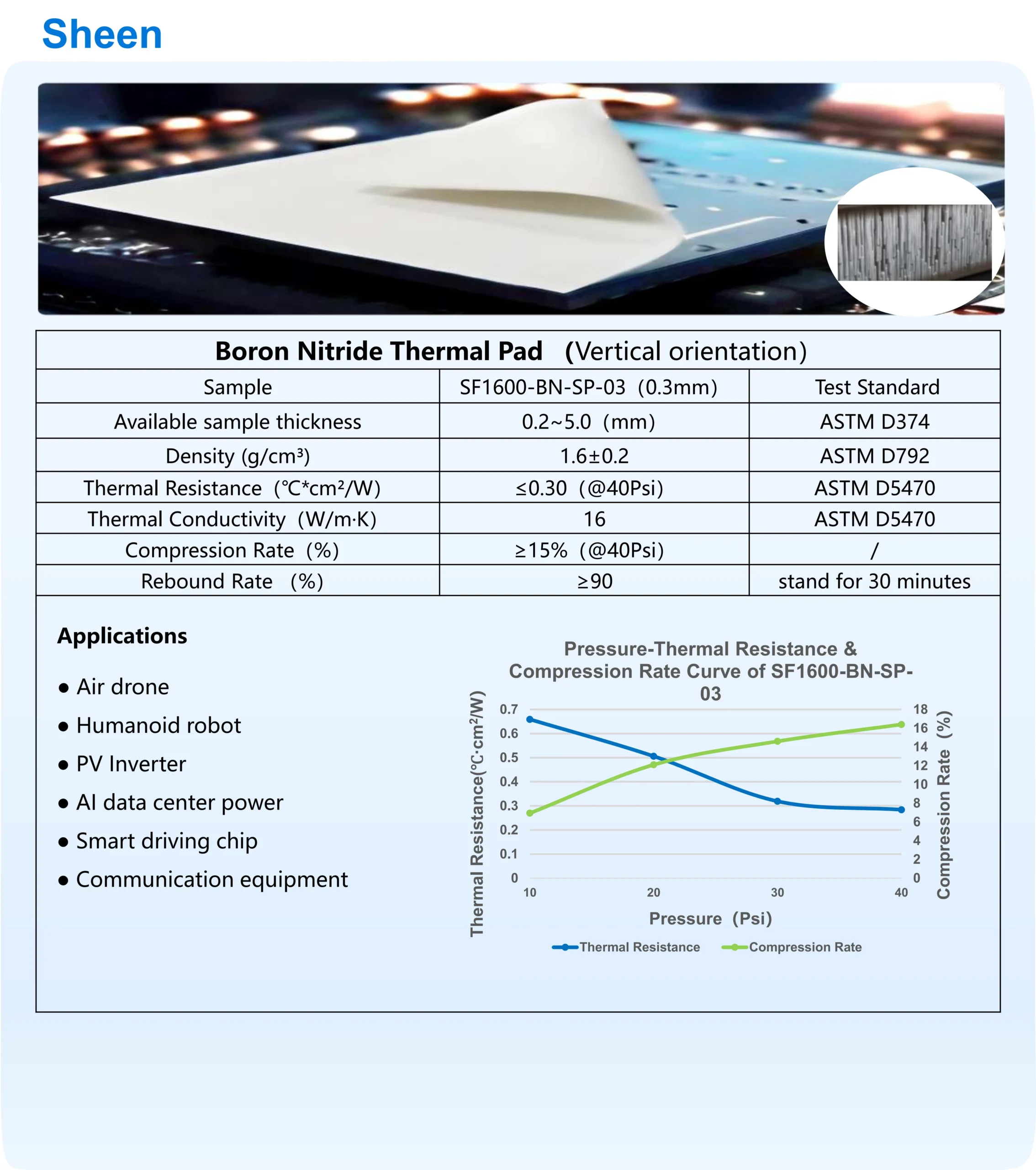
Hexagonal Boron Nitride Pads for Superior Heat Spreading
다음과 같은 경우 Custom-shaped boron nitride pads, the hexagonal boron nitride (hBN structure is the quiet hero. Its layered structure allows strong in-plane 열 방출, turning compact chips into manageable systems.
- High in-plane conductivity
- 전기 절연
- Easy machining into custom BN pads
In practical builds, 열 관리 with hBN often follows this path:
- Map heat source density.
- Design geometry for a tight fit.
- Integrate as a 히트 스프레더 within the stack.
Key performance factors include:
- Material core:
- Crystal orientation
- Purity level
- Pad geometry:
- Thickness tolerance
- Edge shaping
- Interface pairing:
- Contact pressure
- Surface finish
Short takeaway? Smart shaping plus hBN equals efficient 열 패드 that simply get the job done.
Pyrolytic Boron Nitride Pads with High Temperature Stability
For extreme environments, pyrolytic boron nitride (PBN) steps in. This refractory material handles high-temperature cycles while maintaining 열 안정성 and impressive chemical inertness.
Applications often cluster around:
- Semiconductor packaging
- RF cavities
- Vacuum applications
Performance logic unfolds in layers:
- Material deposition ensures ultra-high purity.
- Orientation tuning enhances directional heat flow.
- Precision machining creates custom-shaped BN thermal pads.
Technical stack breakdown:
- Core properties:
- 낮은 가스 배출
- Stable dielectric strength
- Environmental fit:
- Oxidation resistance
- Thermal insulation efficiency
For Custom-shaped boron nitride pads used near plasma or high-frequency modules, PBN keeps cool—literally and electrically.
Ceramic Composite BN Pads Offering Mechanical and Chemical Inertness
A ceramic composite approach blends boron nitride with structural reinforcements, boosting 기계적 강도 그리고 wear resistance. These BN pads act as both heat controllers and durable supports.
Typical advantages:
- Enhanced chemical resistance
- 안정적 dielectric properties
- Long service life as an inert material
Design flow for custom BN pads:
- Select composite ratio.
- Define pad contour for stress points.
- Validate compression and cycling endurance.
Nested performance view:
- Mechanical behavior:
- Compressive load capacity
- Crack resistance
- Environmental stability:
- Corrosion tolerance
- Oxidation delay
- Electrical role:
- Insulation reliability
- Arc resistance
For power electronics, Custom-shaped boron nitride pads in composite form bring toughness without sacrificing thermal control.
Advanced Nitride Ceramic Pads Featuring Anisotropic Thermal Conductivity
현대 nitride ceramic systems push advanced materials engineering further. The highlight? Anisotropic conductivity that enables directional heat transfer.
Core attributes include:
- Tailored crystal alignment
- High dielectric strength
- Integration as a 열 인터페이스 재료
Performance mapping often works like this:
- Define heat flow direction.
- Align ceramic microstructure accordingly.
- Machine into custom-shaped boron nitride pads for tight assemblies.
Layered technical view:
- Thermal behavior:
- In-plane conductivity boost
- Through-plane control
- Structural stability:
- Dimensional precision
- High-performance reliability
- Application fit:
- Compact modules
- Customized thermal solutions
For engineers who want heat guided exactly where it should go, Custom-shaped boron nitride pads built from advanced nitride ceramics are a smart move. Brands like Sheen Technology turn these engineered pads into real-world cooling answers, helping devices stay cooler, safer, and ready for the long haul.
3 Key Benefits Of Custom-Shaped Boron Nitride Pads
Custom solutions are not just hype anymore. When heat rises and circuits get packed tight, Custom-shaped boron nitride pads step in with smart geometry and reliable performance. From thermal control to insulation and strength, these pads quietly keep devices running cool and safe.
Supercharging Heat Dissipation with High Thermal Conductivity
다음과 같은 경우 열 전도성 and fast 열 방출, geometry matters as much as material. Custom-shaped boron nitride pads are designed to sit exactly where heat builds up, cutting down 열 저항 and boosting thermal efficiency.
- Core performance drivers:
- Material advantage
- High intrinsic 열 전도성
- Efficient lateral 열 전달
- Design precision
- Tailored custom geometry
- Close surface contact for better 열 관리
- Application fit
- LED 모듈
- 전력 전자 제품
- Semiconductor packaging
- Material advantage
- Heat source identified
- Pad geometry matched
- Interface pressure optimized
- Cooling solutions enhanced
A well-designed boron nitride pad works like a heat highway. In compact systems, that difference keeps components stable instead of overheating. Sheen Technology refines Custom-shaped boron nitride pads to align material science with real-world layouts, not just lab specs.
Ensuring Electrical Insulation via Exceptional Dielectric Strength
Heat control means nothing without 전기 절연. Custom-shaped boron nitride pads combine high dielectric strength with reliable electrical isolation, helping keep high-current systems safe.
Key protection layers include:
- 높음 항복 전압 for demanding, high voltage applications
- Low dielectric constant to reduce signal interference
- Stable, non-conductive ceramic structure
In practical setups:
- Power modules
- Thermal interface
- Heat flows through
- Electrical path
- Current stays blocked
- Thermal interface
“Advanced electronic packaging in 2025 is increasingly defined by materials that combine thermal performance with electrical safety,” notes a 2025 Yole Group analysis on power electronics substrates.
That balance is why Custom-shaped boron nitride pads are favored in EV converters and industrial drives. With precise shaping, boron nitride pads maintain close contact while preserving electronic protection. Sheen Technology engineers each pad to meet strict insulation demands without sacrificing cooling efficiency.
Maintaining Structural Integrity through Mechanical Stability
Performance fades fast if materials crack or warp. Custom-shaped boron nitride pads stand out for mechanical stability 장기적으로 structural integrity.
Their durability comes from layered advantages:
- Material properties
- 높음 temperature stability
- Strong chemical inertness
- Design customization
- Thickness control
- Edge reinforcement in custom designs
- Operational resilience
- Resistance to compression fatigue
- Stable under repeated thermal cycling
Short and simple: less cracking. Fewer failures. Longer service life.
In harsh environments—chemical processing units, aerospace electronics, heavy industrial drives—boron nitride pads keep shape under pressure. That steady 내구성 supports consistent contact, reliable 열 방출, and safe insulation all at once.
For manufacturers seeking dependable Custom-shaped boron nitride pads, Sheen Technology aligns mechanical stability, precision shaping, and production consistency into one streamlined solution.
Scenario-Based: Power Modules: Custom-Shaped Pads For Cooling
Power modules run hot, and tight layouts leave no room for sloppy thermal control. That’s where Custom-shaped boron nitride pads step in. By combining 열 인터페이스 efficiency, precision fit, and solid insulation, these tailored boron nitride solutions keep 전력 전자 제품 cool, compact, and safe—without overcomplicating the build.
Thermal Interface Pads Tailored for Power Electronics
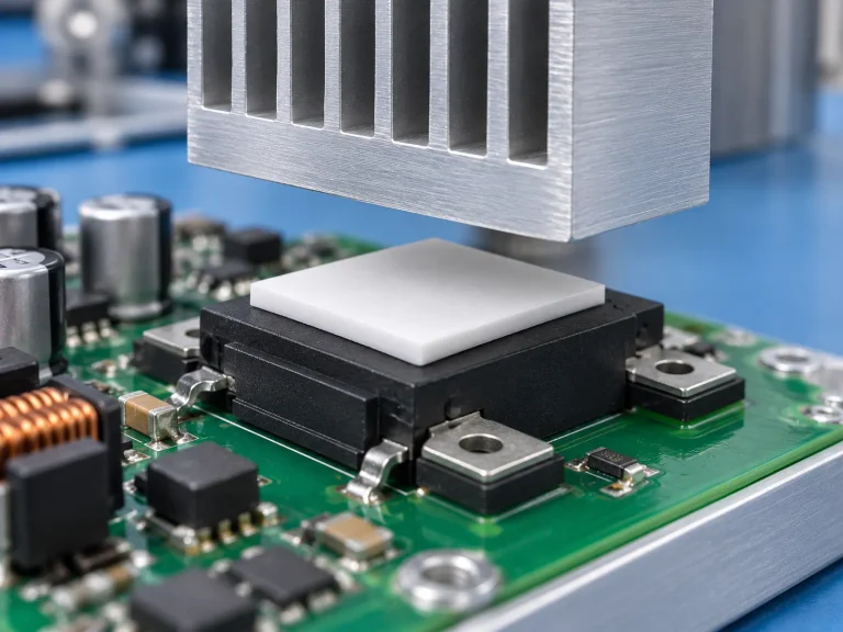
When heat piles up inside 전력 전자 제품, steady 열 방출 becomes non‑negotiable. Custom-shaped boron nitride pads act as high-performance 열 인터페이스 layers, bridging chips and heat sinks with minimal resistance.
Key cooling advantages include:
- High thermal conductivity from boron nitride ceramics
- Gap-filling pads designed for uneven module surfaces
- 신뢰성 냉각 솔루션 in compact assemblies
Performance comparison in typical power modules:
| 재료 유형 | 열 전도성(W/m-K) | Max Temp (°C) | Dielectric Strength (kV/mm) |
|---|---|---|---|
| 실리콘 패드 | 3–6 | 180 | 6 |
| Aluminum Oxide Pad | 20–30 | 250 | 10 |
| Boron Nitride Pad | 30–60 | 800 | 15+ |
In real projects, Custom-shaped boron nitride pads are machined to sit exactly where heat forms—under MOSFETs, IGBTs, or driver ICs. No trimming on-site. No guesswork. Just tight thermal paths and fewer hotspots.
에서 Sheen Technology, custom BN thermal pads are engineered to match load profiles, surface roughness, and airflow conditions, so cooling isn’t left to chance.
Precision Machined Geometries for Tight Module Packaging
밀도 전원 모듈 demand smart precision machining and exact geometries. A generic sheet won’t cut it when every millimeter counts.
- Define thermal and electrical targets within the module design.
- Model the required custom shapes around mounting holes, vias, and copper traces.
- Apply CNC or laser-assisted manufacturing for repeatable tolerances.
Within tight packaging, integration often follows this logic:
- Component Layer
- Semiconductor die
- Substrate
- Solder interface
- Thermal Control Layer
- Custom-shaped boron nitride pads
- Cutouts for fasteners
- Recesses for sensors
- Custom-shaped boron nitride pads
- Mechanical Frame
- Housing
- Compression elements
Short lead times matter. So does dimensional accuracy. Even a 0.2 mm mismatch can reduce contact pressure and hurt 열 방출. That’s why engineered boron nitride pads are delivered ready to drop in—no secondary shaping required.
Electrical Isolators with High Breakdown Voltage in Power Circuits
In high-voltage power circuits, thermal control alone isn’t enough. Strong 전기 절연 is critical.
Electrical isolators made from boron nitride combine thermal flow with high 유전체 강도, protecting sensitive switching nodes from short circuits.
- 높음 항복 전압 supports EV inverters and industrial drives
- Stable performance under thermal cycling
- Clean surface finish for consistent contact
“The push toward higher power density in EV and renewable converters is increasing demand for advanced insulating materials with both thermal and dielectric performance,” notes a 2025 outlook from the International Energy Agency’s power electronics review.
This trend explains the rise of Custom-shaped boron nitride pads in next-gen modules. Engineers want insulation that doesn’t block heat. They want cooling that doesn’t risk arcing.
Sheen Technology delivers Custom-shaped boron nitride pads designed specifically for high-load 전원 모듈, balancing electrical isolators’ performance with efficient thermal paths. In short: cooler systems, safer circuits, and packaging that actually fits.