-
ADD: Building 2, No. 8 Hengzhutang Road, Dongguan
-
Phone: +86 135 4224 3751

Engineering & sourcing support
Thermal Pad Manufacturer for Graphene, Silicone & Gap Filler TIMs
Sheen Materials is a thermal pad manufacturer founded in Dongguan, China in 2005 and manufacturing TIMs in-house since 2008. We produce silicone, non-silicone, graphene, carbon fiber and boron nitride thermal pads from 2 to 130 W/m·K, die-cut from 0.3 mm to 12 mm thick with a minimum die-cut size of 0.2 × 0.2 mm. IATF 16949-certified, and a certified supplier to Henkel, Toyota and Samsung. Send a drawing for a quote — samples ship in 3-5 working days.
- IATF 16949:2016 certified
- 20,000 m² manufacturing plant
- 225 full-time employees
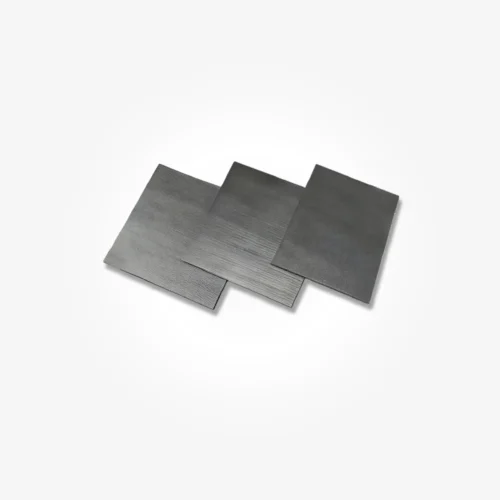
Find your material family
Thermal Pad Types We Manufacture
Six material families cover compliant gap filling, high-performance interfaces and phase change applications. Select the grade against interface thickness, pressure and electrical requirements.
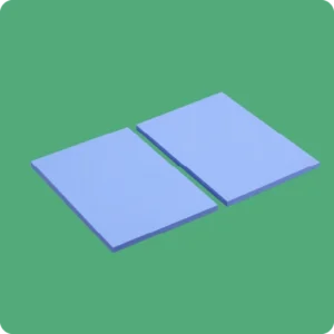
SF series
Silicone Thermal Pads
Compliant SF-series gap fillers for electronics. Select the thickness and hardness for your assembly gap.
Explore silicone pads →
AF series
Non-Silicone Thermal Pads
AF-series pads for silicone-sensitive optical, imaging and automotive assemblies.
Explore non-silicone pads →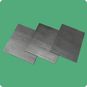
GSF series
Graphene Thermal Pads
GSF-series materials for demanding interfaces, with model-specific through-plane conductivity and thermal resistance data.
Explore graphene pads →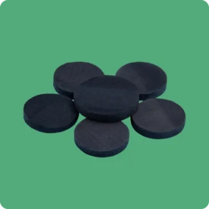
CSF series
Carbon Fiber Thermal Pads
CSF-series pads for high-performance electronics, matched to interface geometry and electrical requirements.
Explore carbon fiber pads →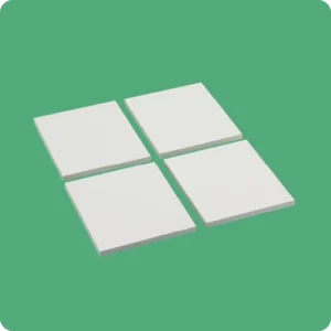
Boron nitride materials
Boron Nitride Thermal Pads
Boron nitride pads combining thermal performance and electrical insulation, with grade-specific dielectric data.
Explore BN pads →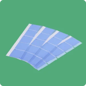
SP205A series
Phase Change Materials
SP205A-series materials for thin CPU, GPU and other flat interfaces.
Explore phase change TIMs →From your drawing to an assembly-ready part
Custom Thermal Pad Manufacturing Capabilities
Every part is made to your drawing: thickness from 0.3 mm to 12 mm, minimum die-cut size 0.2 × 0.2 mm (achievable dimensions depend on material hardness and thickness), with adhesive lamination, release liners, sheet and roll supply, and custom tooling for irregular outlines, cut-outs and multi-cavity layouts.
Custom shapes
Irregular outlines, cut-outs and multi-cavity layouts.
Thickness & fit
0.3 mm to 12 mm, matched to gap tolerance and compression.
Handling options
Adhesive lamination and release liners for part placement.
Supply formats
Cut parts, sheet and roll supply, and project packaging.
Supplier qualification
Certifications & Test Reports
Sheen Materials is an IATF 16949:2016-certified thermal pad manufacturer and a certified supplier to Henkel, Toyota and Samsung. Documentation for your qualification file is listed below.
Management System Documents
IATF 16949:2016 — NQA Certificate No. T179463; IATF Certificate No. 0466349.
ISO 9001:2015 — Certificate No. 94126Q00071R301.
ISO 14001:2015 — Certificate No. 04126E0007R001.
Copies available on request for your supplier qualification file.
Compliance & Flammability Reports
Our silicone thermal pads, including grade SF1200, are UL 94 V-0 rated — tested by YCCT, Report No. YCCT512021102605RY01. Materials are RoHS compliant, verified by CTI (Centre Testing International), Report No. A2260351200101001E.
Request applicable reports →Datasheets & Test Conditions
Review the selected grade’s thermal, electrical and mechanical data. Independent material testing by CTI, Report No. A2250540950101001E.
Browse datasheets →Request certificate copies, test reports and datasheets for your supplier qualification file.
Request a Documentation Pack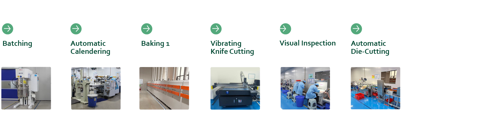
Manufacturing in Dongguan, China
Our Factory & Production Processes
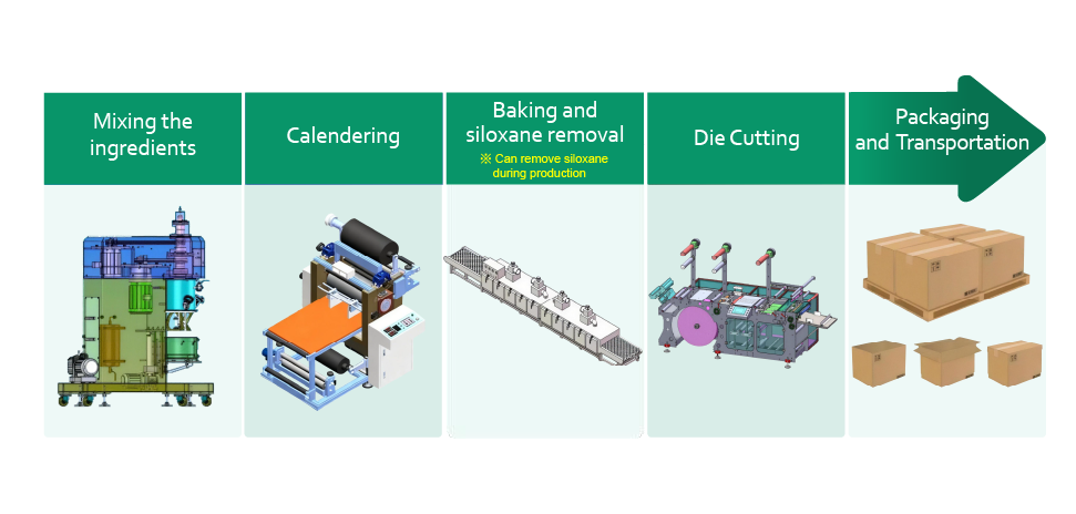
Founded in 2005 as a thermal materials trading company, Sheen began manufacturing in-house in 2008, starting from a 400 m² facility with 15 employees. Today we operate a 20,000 m² plant with 225 full-time employees, covering compounding, calendering, die-cutting and QC.
- Material preparation and forming processes
- Cutting and converting for part geometry
- Inspection against agreed specifications
- Packaging and shipment planning for your project
Standard orders ship in 7-10 working days after sample approval. Every batch is tested for thermal conductivity, thickness and material consistency, with traceability records retained for automotive and medical customers.
Explore Our Production Processes →Evaluate the complete interface
Thermal Performance & Quality Verification
Compare installed thermal performance, compression and insulation alongside conductivity. Use the same test conditions when comparing candidate grades.
| Selection parameter | What to review for your application |
|---|---|
| Thermal conductivity | Grade, measurement method and direction; use through-plane data for heat flow across pad thickness. |
| Thermal resistance | Test thickness, contact pressure and surface conditions, including any adhesive layers. |
| Thickness & compression | Nominal thickness, tolerance, working gap and available assembly force. |
| Electrical properties | Insulation requirements, dielectric data and exposed conductive edges. |
| Operating environment | Operating temperature, cycling, contamination sensitivity and reliability targets. |
| Inspection & documentation | Critical dimensions, acceptance criteria and batch documentation. |
Application-driven selection
Thermal Pads for Electronics & Power Applications
Materials for electronics, communications and power conversion, selected around each assembly’s thermal path.
AI Servers & Accelerators
Low-resistance interfaces around processors, memory and power components.
Server applications →Optical Modules
Compact interfaces with insertion and contamination-control requirements.
Optical module applications →Automotive Electronics
Thermal interfaces with defined tolerances, insulation and qualification needs.
Automotive applications →Energy Storage & BESS
Gap filling and insulation for modules, power conversion and control assemblies.
Energy storage applications →PV Inverters & Power Electronics
Thermal and electrical requirements around power conversion components.
Inverter applications →Industrial & Connected Equipment
Constrained thermal paths in telecom, industrial and connected electronics.
Explore all applications →A practical sourcing process
From Project Requirements to Production
A defined interface and approved specification guide the project from sampling to production.
Share Requirements
Send your drawing, gap, quantity, destination and thermal or electrical targets.
Review Material Options
Select candidate grades, construction and documentation for the quotation.
Evaluate Samples
Validate fit, handling and thermal performance in your assembly.
Plan Production
Approve the part, packaging, inspection criteria and delivery schedule.
MOQ is USD 500 in order value, with no minimum quantity per part number. Samples ship in 3-5 working days after drawing and material confirmation. Production lead time is 7-10 working days for standard orders.
Thermal interface basics
What Is a Thermal Pad?
A thermal pad is a thermally conductive interface material placed between a heat-generating component and a heat sink, cold plate or enclosure. It replaces air in the interface; compliant grades also accommodate the designed gap between mating surfaces.
Pre-cut pads provide defined shapes for assembly. Material selection depends on thickness, contact pressure, electrical properties and the operating environment.
Choose a thermal pad manufacturer that supports both material performance and your required geometry, documentation and production volume.
Browse Thermal Pad Options →Engineering & purchasing questions
Frequently Asked Questions
What information do you need for a thermal pad quotation?
Send your drawing or dimensions, thickness, quantity and destination, plus thermal, electrical, adhesive and packaging requirements.
What is your minimum order quantity?
MOQ is USD 500 in order value. There is no minimum quantity per part number, so mixed part numbers can be combined to reach it.
Can I request samples before placing a production order?
Yes. Samples ship in 3-5 working days after drawing and material confirmation. Contact us on sample charges; tooling is credited on repeat orders.
How long does custom thermal pad production take?
7-10 working days for standard orders, after sample approval.
Can you manufacture thermal pads to my drawing?
Yes. We offer custom outlines, cut-outs and tooling. Thickness ranges from 0.3 mm to 12 mm; minimum die-cut size is 0.2 × 0.2 mm, depending on material hardness and thickness.
Do you offer non-silicone thermal pads?
Yes. AF-series non-silicone pads serve silicone-sensitive optical, imaging and automotive applications.
What thermal conductivity should I specify?
Our range covers 2 to 130 W/m·K. Start with the heat path, interface gap, available contact pressure and target thermal performance. Compare model-specific data and test conditions. A higher conductivity value alone does not establish the lowest installed thermal resistance.
Can thermal pads be supplied with adhesive?
Yes, subject to material and construction. Specify the required side and bonding surfaces; account for adhesive thickness and thermal resistance.
Which certificates and compliance reports can I request?
IATF 16949:2016 (NQA T179463 / IATF 0466349), ISO 9001:2015 (94126Q00071R301), ISO 14001:2015 (04126E0007R001). Silicone pads including SF1200 are UL 94 V-0 rated — tested by YCCT (Report No. YCCT512021102605RY01). Materials are RoHS compliant, verified by CTI (Report No. A2260351200101001E).
Can you support OEM packaging or custom supply formats?
Yes. OEM/ODM options include private-label packaging, sheet and roll supply, and custom converted parts.
Start your material review
Request a Thermal Pad Quote
Send your drawing, material requirements and target volume for a quotation. MOQ starts at USD 500; samples ship in 3-5 working days after drawing and material confirmation.
Need selection support? Include the interface gap, contact pressure and insulation requirements.
For technical selection, you can also contact our technical support team.
- Application & interfaceDevice, heat source and mating surfaces
- Drawing & dimensionsPart shape, thickness and gap tolerance
- Performance requirementsThermal targets, contact pressure and insulation needs
- Quantity & deliverySample quantity, production volume and destination
- Additional requirementsAdhesive, liners, packaging and qualification documents