
Camera FPGA Thermal Dissipation and Optical Cleanliness Solution
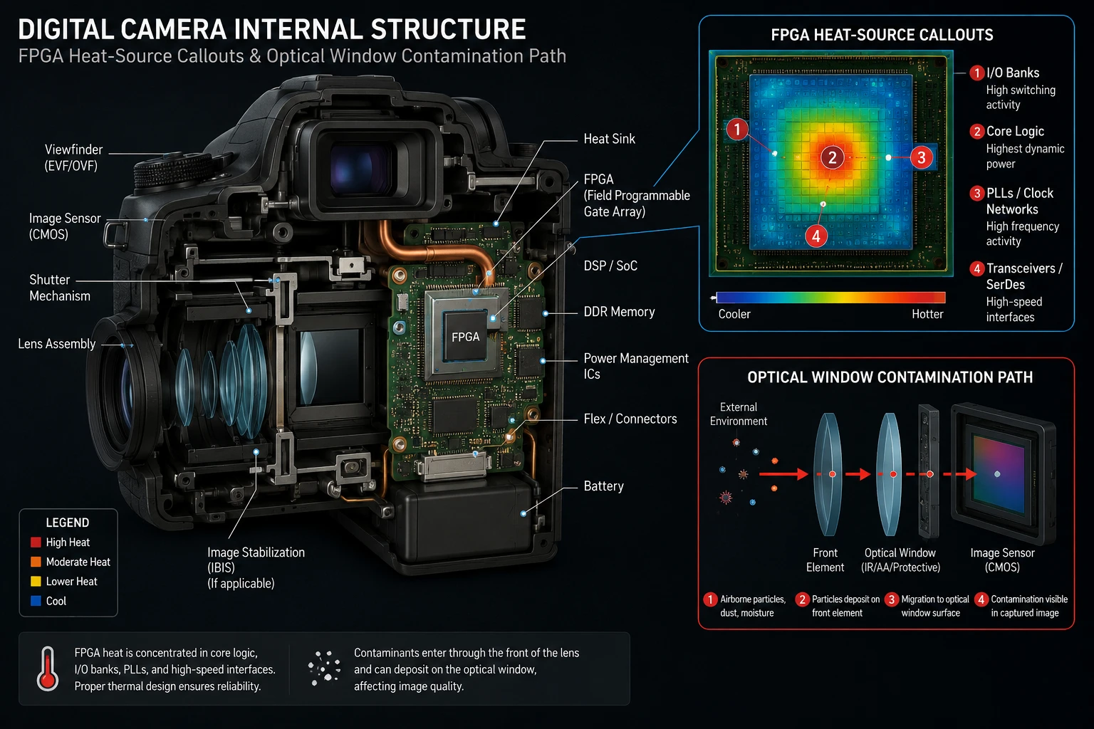
This page addresses a camera assembly in which an FPGA operates at 55–70°C while the optical window remains sensitive to volatile residue from conventional silicone-based thermal interface materials.The design objective is to maintain a stable thermal path from the FPGA to the heat sink or housing, while reducing the risk of silicone-related deposition on optical surfaces over long operating periods.
Application Scenario Overview
Project Background and Application Context
The target assembly combines a localized FPGA heat source with a contamination-sensitive optical path. Material selection therefore cannot be based on conductivity alone; outgassing behavior, gap compliance, interface pressure, and long-term cleanliness must all be evaluated together.
Application Context
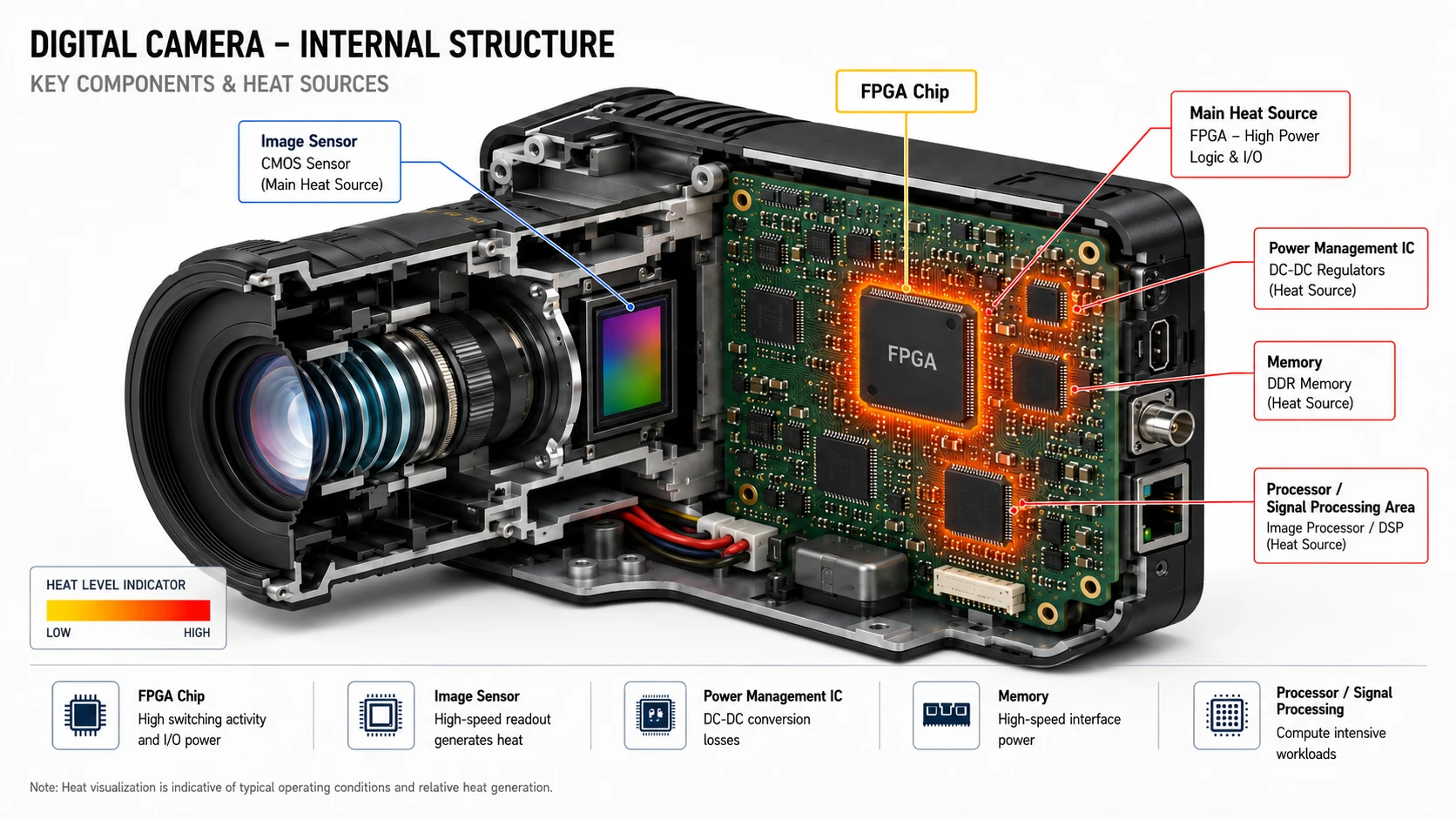
The FPGA runs continuously at 55–70°C and must transfer heat into the mechanical cooling structure without introducing residues that could condense on the optical window or nearby sensor-side surfaces.
- Primary heat source: FPGA processor
- Nominal operating range: 55–70°C
- Nominal interface gap: 0.8 mm
- Primary design target: controlled thermal path with low contamination risk
Heat Sources / Structural Pain Points
Main Thermal and Contamination Challenges in This Camera
This section defines the coupled constraints that drive material selection: localized FPGA heat generation, limited interface gap, and the need to prevent condensable volatile species from reaching the optical path.
Why the Existing Silicone Pad Became a Risk
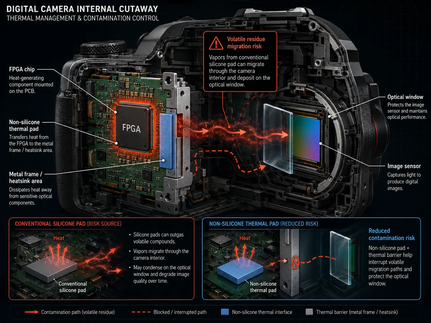
In silicone-based pads, low-molecular-weight siloxanes can migrate when the interface is exposed to sustained temperature and clamping stress. The issue is not only bulk thermal performance, but also material stability under real assembly conditions.
Once released, these species can move through the internal cavity and condense on colder optical window surfaces, forming a thin residue layer that is difficult to remove in service.
At the system level, that residue can degrade image quality, change optical transmission, and create a latent reliability issue even when the FPGA temperature itself remains within the acceptable range.
For this reason, the thermal interface in this design must be assessed for both heat-transfer function and contamination behavior over the intended operating life.

Recommended Material Combination
Recommended Material Selection for the Camera FPGA Application
For a nominal 0.8 mm interface and an FPGA operating range of 55–70°C, AF500 and AF600 are practical starting points for engineering validation. The choice between them depends on required thermal margin, compression behavior, and acceptable cost/performance tradeoff.
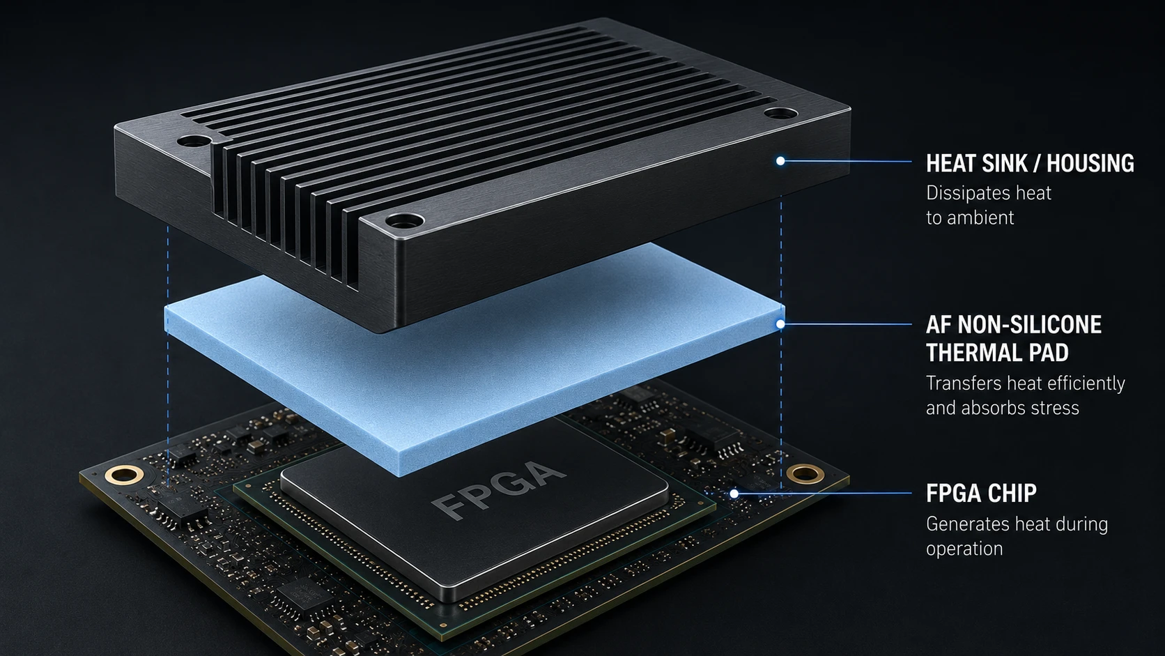
Heat Source: FPGA
Gap: 0.8 mm
Material Candidates: AF500 / AF600
Target: Thermal Control + Optical Cleanliness
AF500
Thermal conductivity: 3.0 W/m·K. Recommended evaluation thickness: 0.8 mm or 1.0 mm. Suggested compression ratio: 15%–25%.
Use AF500 when the heat load is moderate and the program requires a balanced starting point for thermal performance, cleanliness control, and material cost.
Download AF500 PDF →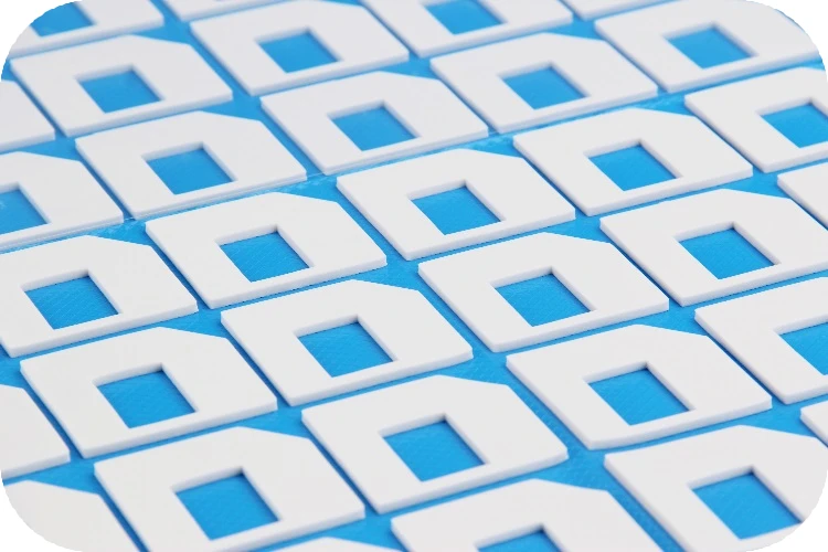
AF600
Thermal conductivity: 5.0 W/m·K. Recommended evaluation thickness: 0.8 mm or 1.0 mm. Suggested compression ratio: 15%–25%.
Use AF600 when lower interface thermal resistance and higher temperature margin are required, especially for longer duty cycles or tighter thermal budgets.
Download AF600 PDF →
AF Series Selection Basis
AF Series removes silicone oil from the material system and is therefore relevant to designs where contamination risk matters as much as gap filling and heat transfer.
View AF Series →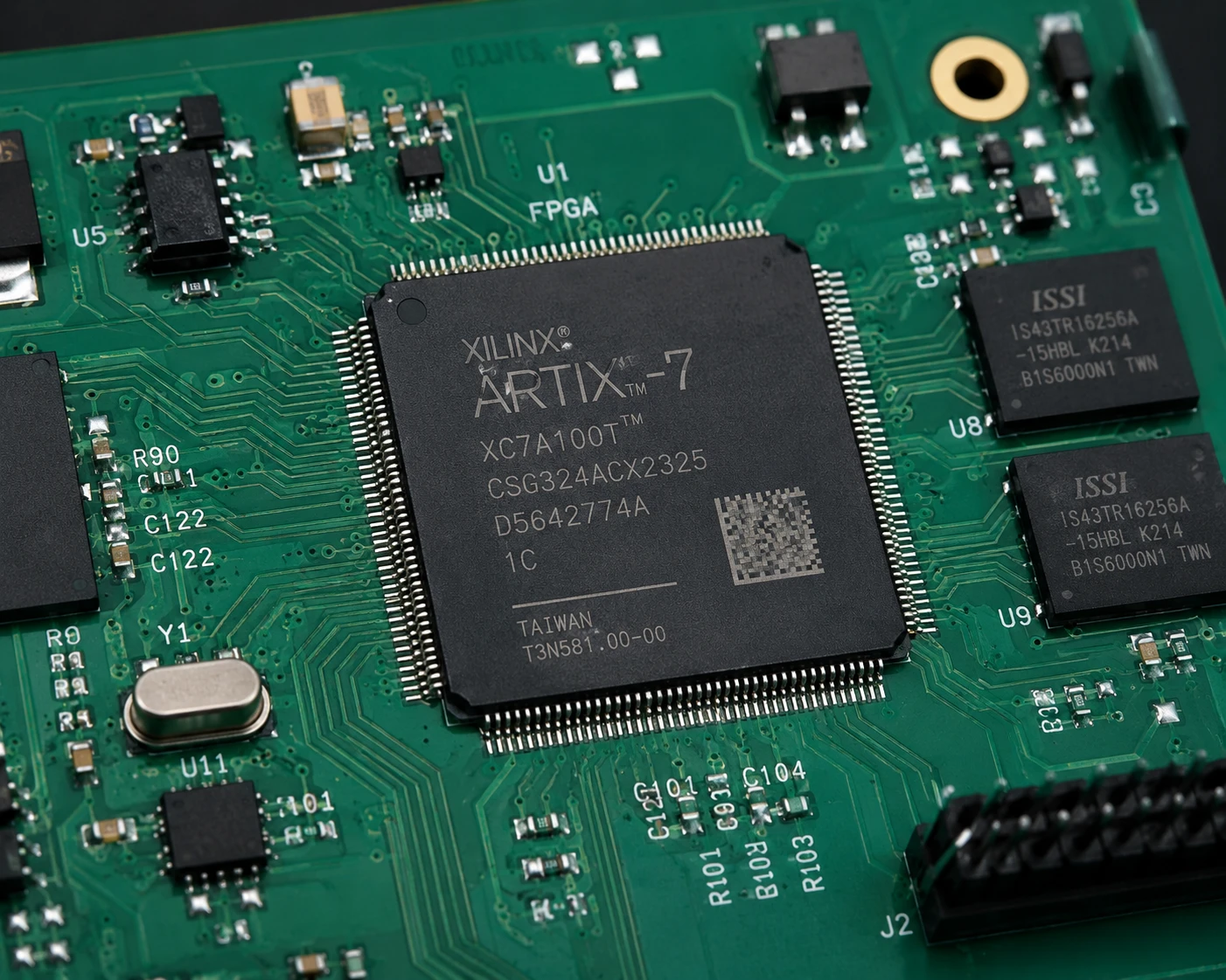
Initial Recommendation
Start with AF600 when thermal margin is the primary concern. Use AF500 as a comparison sample when the assembly has lower heat flux or when the program needs a lower-cost baseline for validation.
See validation plan →Why Choose This Solution
Why the AF Non-Silicone Solution Fits This Camera Application
This section explains the engineering basis for selecting an AF non-silicone thermal pad in this camera design, focusing on contamination control, heat-transfer capability, interface reliability, and long-term assembly stability.
Eliminate Fogging Risk at the Source
The non-silicone material system reduces the probability of low-molecular siloxane migration and therefore lowers the risk of residue deposition on the optical window.
Fully Cover the Thermal Requirement
AF600 at 5.0 W/m·K provides a practical path for reducing FPGA-to-sink interface resistance while maintaining conformability across the 0.8 mm gap.
Comprehensive Reliability Assurance
Electrical insulation, flame retardancy, gap compliance, and long-term material stability can be evaluated within the same candidate family rather than mixing multiple interface concepts.
Life-Cycle Cost Advantage
A contamination-stable interface can reduce rework, service risk, and inspection burden even when the initial material cost is higher than a standard silicone pad.
Implementation Points
Implementation Logic in the Real Camera Structure
This section translates the material choice into assembly-level considerations, including cleanliness control, gap tolerance, contact stability, and practical integration into the camera structure.
Clean Optical Window
The thermal interface should not release condensable species that could accumulate on the optical window during long-term operation.
Read FAQ →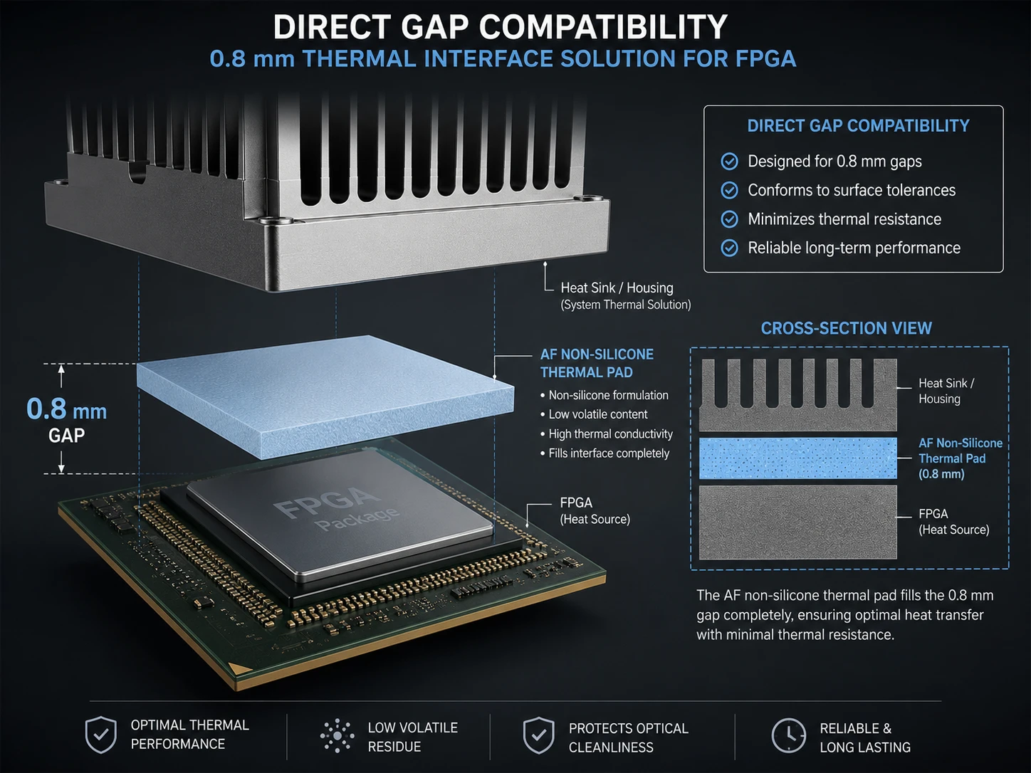
Direct Match to 0.8 mm Gap
AF Series can be evaluated at 0.8 mm or 1.0 mm thickness, allowing direct comparison between nominal gap match and controlled compression allowance.
Review selection →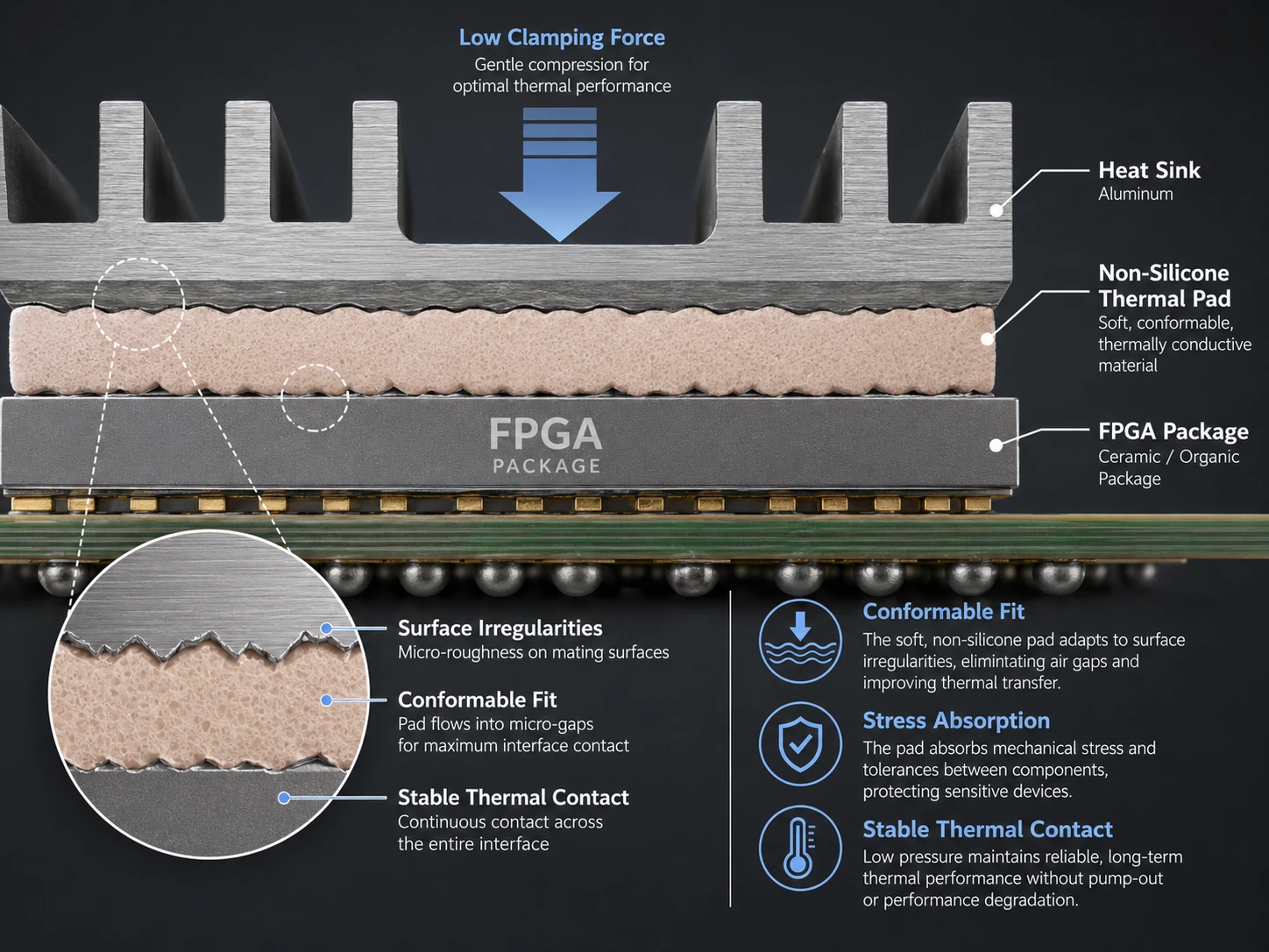
Compression-Friendly Interface
The pad must maintain contact under practical clamp load without creating excessive mechanical stress on nearby optical or PCB structures.
See validation →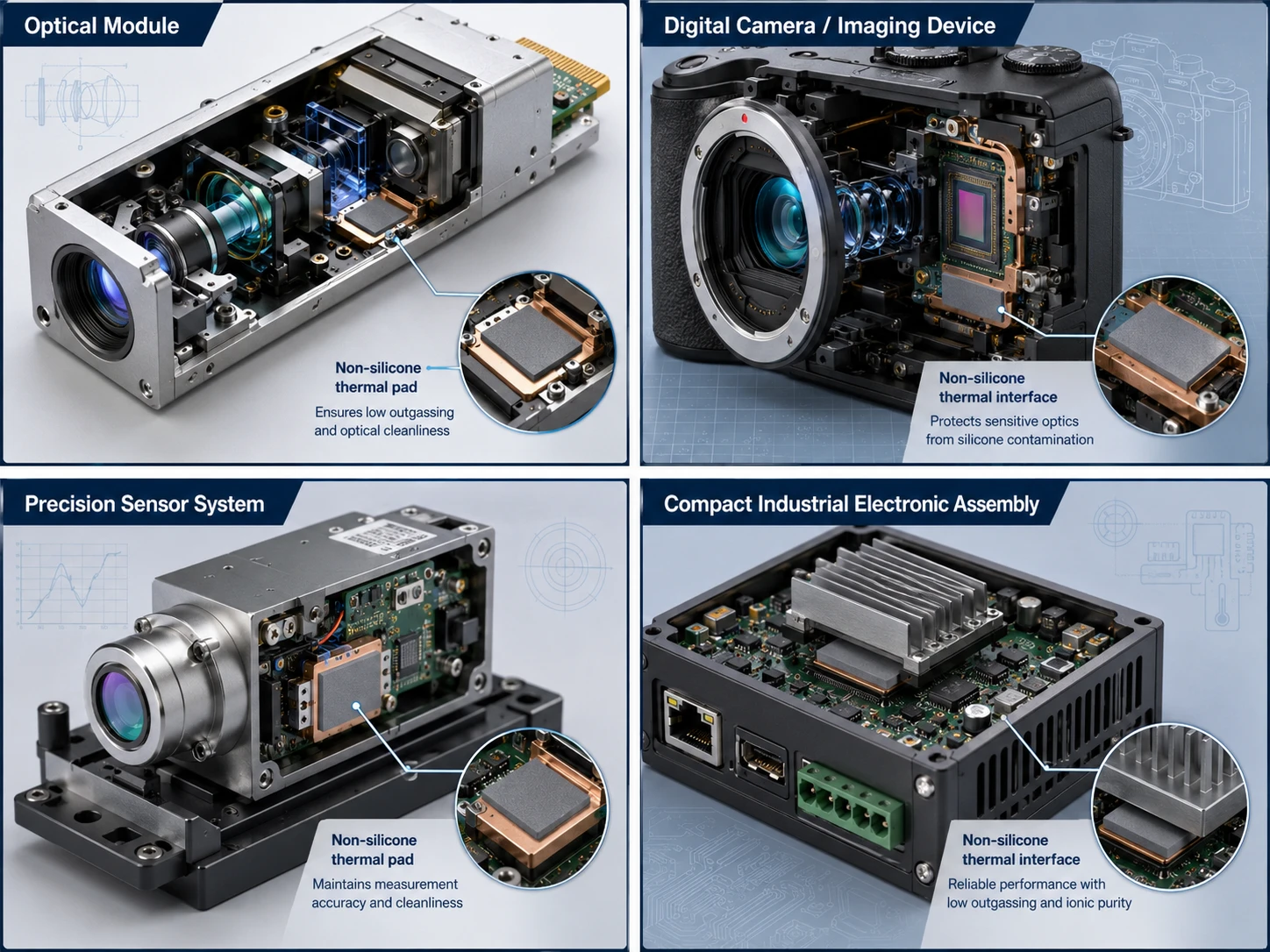
Reference Application Background
Similar non-silicone interface concepts are relevant to other contamination-sensitive assemblies where optics and electronics share a confined enclosure.
Get engineering support →Testing / Validation Evidence
Suggested Sample Validation and Implementation Steps
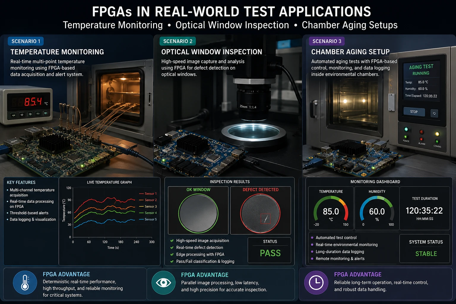
Validation should confirm both thermal function and contamination behavior in the real assembly. The recommended test flow therefore includes temperature monitoring, optical inspection, insulation checks, and long-duration aging under representative loading.
Validation Checklist
- Prepare AF500 and AF600 samples in 0.8 mm thickness for side-by-side evaluation.
- Replace the original silicone pad and run continuous operation at 55–70°C for at least 500 hours.
- Periodically inspect the optical window glass for oil film or fogging and compare with a silicone-pad control group.
- Record FPGA temperature-rise and steady-state temperature under different operating conditions.
- Verify insulation performance, compression rebound condition, and interfacial fit after long-term operation.
- If possible, extend testing to 500–1000 hours at 70°C chamber condition to monitor optical cleanliness, chip temperature trend, and thermal stability.
FAQ
Common Questions
These questions address the main engineering concerns for this design: conductivity versus real interface performance, gap adaptation, long-term reliability, insulation margin, and practical selection logic between AF500 and AF600.
Will 5.0 W/m·K be enough?
For this operating range, AF600 is a reasonable validation candidate. Final suitability should be confirmed from measured FPGA temperature, interface pressure, and contact quality in the assembled structure.
Can a non-silicone pad match a 0.8 mm gap?
Yes. AF Series can be evaluated at nominal 0.8 mm thickness or with a small positive thickness offset, depending on the target compression ratio and the flatness of the mating surfaces.
What matters more than conductivity alone?
For this application, outgassing behavior, compressibility, contact resistance, and long-term stability are at least as important as bulk thermal conductivity.
Is the insulation performance reliable enough?
The candidate material should be verified against the electrical spacing and insulation requirements of the actual camera PCB and housing configuration. Datasheet values are only the starting point.
When should AF500 be preferred over AF600?
AF500 is useful as a baseline option when the heat load is moderate and cost sensitivity is higher. AF600 is better when lower interface thermal resistance and more temperature margin are needed.
What is the key engineering decision here?
The main decision is whether the camera design should prioritize lowest initial material cost or a lower-risk interface that addresses both thermal control and optical cleanliness over service life.