-
АДД: Здание 2, № 8 Хэнчжутан Роуд, Дунгуань
-
Телефон: +86 135 4224 3751

The Future of Optical Module Thermal Management in AI Data Centers
With the rapid advancement of Artificial Intelligence (AI) technology, AI data training and applications frequently entail massive data transmission and real-time interaction, leading to an explosive surge in demand for both computing power and network infrastructure.
As the “couriers” responsible for transmitting data between devices within a network, optical modules facilitate the reception and transmission of vast quantities of data across the “computing power highway”; consequently, their critical importance is becoming increasingly evident.
Optical modules are pivotal components in the era of AI computing power. However, as transmission speeds continue to escalate—progressing from 400G to 800G, 1.6T, 3.2T, and eventually 6.4T—the power consumption of these modules is also rising exponentially. Consequently, thermal management has emerged as a significant limiting factor hindering the further development of optical modules.
Today, let us take a closer look at the specific internal structure of optical modules and explore how best to address the critical challenge of thermal management.
What Is an Optical Module?
Optical modules serve as the “signal translators” of fiber-optic communication systems. Their core function is to convert electrical signals—emitted by devices such as servers, switches, and base stations—into optical signals capable of high-speed transmission through optical fibers.
Upon reaching their destination, they convert these optical signals back into electrical signals, thereby enabling “electrical-to-optical-to-electrical” signal conversion as well as long-distance and high-capacity data transmission.
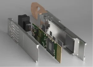
Simply put, an optical module is a key device that performs the conversion of optical and electrical signals, serving as a core component within optical communication systems.
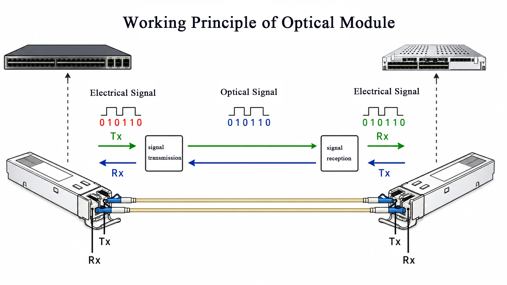
The two most critical components within an optical module are its core chips: the “optical chip” and the “electrical chip.” The optical module functions by relying on the collaborative division of labor between these two key players to facilitate the “electrical-to-optical-to-electrical” signal conversion and transmission process.
Currently, in the low-end optical chip sector—specifically for speeds below 10 Gb/s—China has achieved a high level of maturity in both R&D and manufacturing.
However, in the high-end optical chip and component sector—covering speeds of 25 Gb/s and above—a significant gap remains when compared to the world’s leading enterprises. Furthermore, high-end electrical chips—particularly DSP chips—remain largely monopolized by companies such as Broadcom and Marvell.
The “optical chip” serves as the “heart” of an optical module; it primarily comprises components such as lasers, detectors, couplers, connectors, and filters. These elements are integrated within the TOSA (Transmitter Optical Sub-Assembly) and ROSA (Receiver Optical Sub-Assembly) to facilitate electrical-to-optical conversion (at the transmitting end) or optical-to-electrical conversion (at the receiving end).
“Electrical chips” primarily comprise driver chips, receiver chips, and Digital Signal Processing (DSP) chips. Located on the optical module’s PCB, these components function as independent small chips in low-speed modules; in high-speed modules, they can be integrated with the DSP to process electrical signals, thereby performing functions such as signal driving, amplification, encoding, decoding, compensation, and clock recovery.
Where are the heat sources located within an optical module?
The primary sources of heat generation in an optical module lie within its two major components: the “optical chip” and the “electrical chip.” Specifically, the key heat-generating points include the optical chip’s lasers, detectors, couplers, connectors, and filters, as well as the electrical chip’s driver chips, receiver chips, and Digital Signal Processing (DSP) chips.
The heat generated by optical modules primarily originates from the “electrical-to-optical conversion” and “signal processing” stages; the core heat sources are concentrated within three key components. Furthermore, as data rates increase (e.g., to 1.6T or 3.2T), the heat generation becomes more concentrated, and the demand for effective heat dissipation becomes increasingly urgent.
(1) The Primary Heat Source — The Transmitter (TX): Laser Diode (LD)
Causes of Heat Generation: The laser serves as the core component for “converting electricity into light.” It generates laser output by means of electrical current drive; the current density involved is extremely high (reaching up to 10 kA/cm² in high-speed modules). Only 30–50% of the electrical energy is converted into light energy, while the remainder is entirely converted into thermal energy.
Heat Generation Intensity: Accounts for 40–60% of the module’s total power consumption; for 1.6T optical modules, the power consumption of the lasers reaches 12–18 W, with localized heat flux densities exceeding 50 W/cm² (far surpassing the limits of air cooling).
The Necessity of Heat Dissipation: The junction temperature of the laser must be strictly maintained at ≤85°C (as established in the core thresholds mentioned previously). Exceeding this temperature limit leads to wavelength drift (at a rate of 0.1 nm/°C) and a degradation of laser output power, thereby directly impacting the communication bit error rate (which must remain ≤10⁻¹²).
(2)The Second Largest Heat Source—Control Unit: DSP Chip
Cause of Heat Generation: The DSP chip acts as a “signal conditioner,” responsible for encoding/decoding, signal compensation, and rate adaptation (such as high-speed signal processing for 800G/1.6T); it involves massive computational loads, and its power consumption increases exponentially with the data rate.
Heat Generation Intensity: Accounts for 25–40% of the module’s total power consumption; the 800G DSP chip consumes approximately 8–12 W, while the 1.6T DSP chip reaches 10–15 W, resulting in a chip surface heat flux density exceeding 30 W/cm².
Thermal Management Necessity: The maximum junction temperature limit for DSP chips is 105°C. Exceeding this threshold triggers thermal throttling (automatic rate reduction) or even system shutdown, resulting in interconnect disruptions within AI clusters and data centers.
(3)Auxiliary Heat Source — Receiver (RX): Photodetector + TIA Chip
Cause of Heating: The TIA (Transimpedance Amplifier) is responsible for amplifying the faint electrical signals received by the photodetector (PD). In high-speed scenarios (such as 800G or 1.6T), the requirement for high-bandwidth amplification generates additional heat.
Heat Generation Intensity: Accounts for 10–20% of the module’s total power consumption; while the overall heat flux density is lower than that of the lasers and DSP, localized hotspots may still form.
Necessity of Heat Dissipation: The junction temperature of the TIA chip must remain ≤ 95°C; exceeding this limit leads to signal amplification distortion, impairs receiver sensitivity, and consequently reduces the transmission distance.
Optical Module Heat Dissipation Solutions
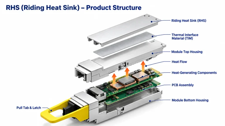
Optical modules are enclosed, compact packages (such as QSFP-DD/OSFP) where heat must be dissipated through specific regions; these two regions constitute the core of the thermal design:
Module Top / Bottom Heat Dissipation Surfaces (Interface with External Heat Dissipation Structures)
1.1 Function: The top or bottom of the module housing (typically aluminum alloy) is designed as a “heat dissipation contact surface,” which must make firm contact with the switch’s heat sink, cold plate (for 1.6T+ modules), or air-cooling channel.
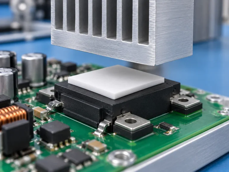
1.2 Key Requirements: The flatness tolerance of the contact surface must be ≤ 0.1 mm, and the surface roughness Ra must be ≤ 1.6 μm; otherwise, air gaps will form (resulting in a sudden spike in thermal resistance). In such cases, a thermal pad (TIM material) must be used as a filler to ensure that the interfacial thermal resistance remains ≤ 0.1 ℃·in²/W (per the previously cited standard).
1.3 Speed Differences: 800G and lower-speed modules rely on heat exchange between their top heat dissipation surfaces and air-cooling channels, whereas 1.6T+ modules require direct contact between their bottom heat dissipation surfaces and a cold plate (making liquid cooling a mandatory requirement).
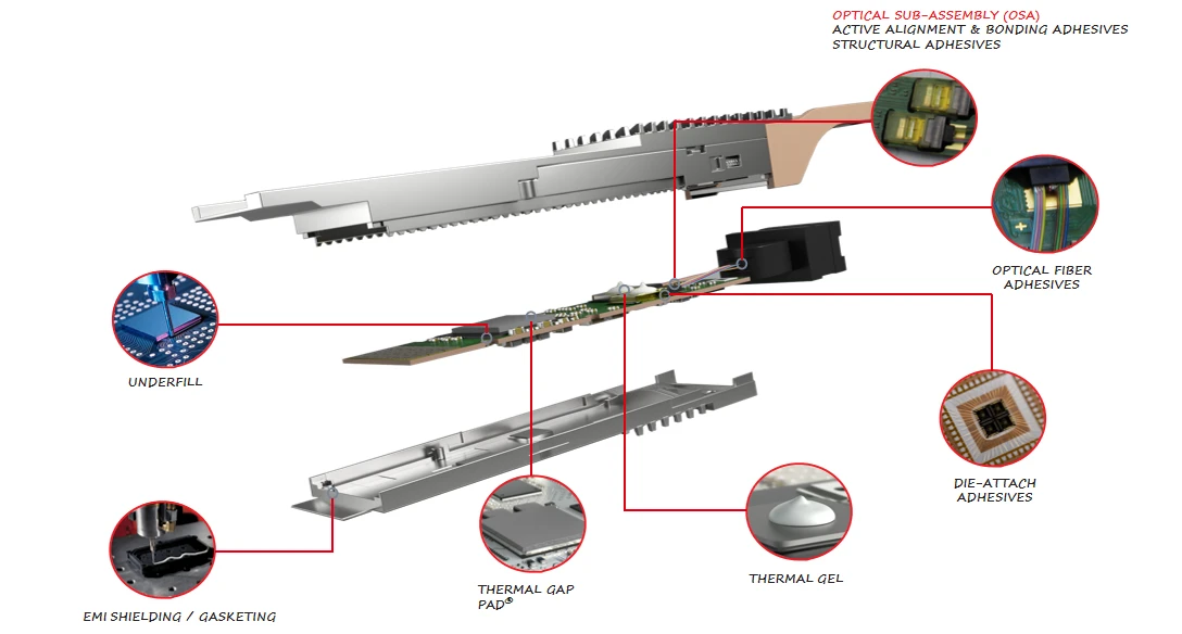
Internal Thermal Conduction Path (Conduction Channel from Heat Source to Enclosure)
2.1 Function: By utilizing internal thermal conduction structures (such as copper substrates or micro heat spreaders), heat generated by the laser and DSP chip is rapidly transferred to the housing, thereby preventing the accumulation of localized hot spots.
2.2 Key Design Elements:
- Lasers and DSP chips must be mounted directly onto a high-thermal-conductivity substrate (copper or ceramic, with a thermal conductivity of ≥300 W/m·K);
- Thermal gel (with a thermal conductivity of ≥6 W/m·K) must be applied between the chips and the substrate to eliminate microscopic gaps.
- 1.6T+ modules require an integrated miniature heat spreader to distribute localized heat flux densities of 50 W/cm² across the entire housing, thereby mitigating thermal concentration stress.
Naturally, thermal management solutions vary significantly depending on the transmission rates of the optical modules in question.
| Data Rate | Heat Flux Density | Recommended Thermal Solution | Key Configuration Points | Suitable Scenarios |
|---|---|---|---|---|
| 10G/25G | < 5W/cm² | Pure passive cooling | Aluminum housing + copper shim + thermal gel | Enterprise campus networks, FTTH broadband access |
| 400G | 10–15W/cm² | Passive cooling + optimized air cooling | High-thermal-conductivity substrate + housing heat-dissipation fins + directional fan | Traditional data centers, telecom metro networks |
| 800G | 15–25W/cm² | Active air cooling for high-end applications / liquid cooling for AI scenarios | Vapor chamber + turbo fan; or heat pipe + cold plate | Standard server rooms with air cooling, AI inference clusters with liquid cooling |
| 1.6T | 30–50W/cm² | Direct liquid cooling with floating cold plate / hose | Built-in vapor chamber + bottom cold plate contact + metal corrugated tube | Intelligent computing centers, AI training clusters |
| 3.2T+ | ≥50W/cm² | Immersion liquid cooling / CPO discrete liquid cooling | Vapor chamber + turbo fan, or heat pipe + cold plate | Supercomputing centers, next-generation AI clusters |
As the Technical Editor-in-Chief at Материалы для отделки, Kevin Kan observes that passive cooling remains the predominant thermal management strategy for optical modules today. The most critical material utilized in the passive cooling of optical modules is a high-conductivity материал теплового интерфейса—specifically, thermal gel.
Consequently, the requirements for thermal gels used in optical modules have increased significantly, necessitating a thermal conductivity of at least >12 W/(m·K). Furthermore, stringent standards must also be met regarding low volatility, curing time, reliability, and durability.
This presents both an opportunity and a challenge for many manufacturers of thermal interface materials. Currently, a number of manufacturers have already released high-conductivity thermal gel solutions specifically tailored for optical modules.
Материалы для отделки offers a comprehensive, systematic, and professional suite of thermal management solutions for optical modules; for the 2025–2026 period, the company is already supplying thermal products to at least three large-scale optical module enterprises, generating an annual production value exceeding $20 million.
Материалы для отделки is a high-tech enterprise based in Dongguan, China, specializing in the R&D and manufacturing of advanced thermal management materials and functional materials, such as foamed silicone. The company operates a 13,000-square-meter facility and employs a workforce of over 200 people. With 18 years of deep expertise in the field of thermal interface materials, Sheen Materials offers a comprehensive product line that includes graphene thermal pads, carbon fiber thermal pads, boron nitride thermal pads, thermal silicone pads, thermal grease, thermal gels, non-silicone thermal pads, phase-change thermal materials, and foamed silicone.
Материалы для отделки has developed a series of advanced thermal interface materials—backed by independent intellectual property rights—tailored for sectors such as high-power AI chips, 5G communication equipment, data centers, autonomous driving systems, consumer electronics, and power and energy storage systems.
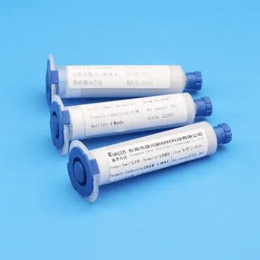
Sheen’s SE120 Thermal Gel 12.0W/mK
Sheen SE120 Thermal Gel is a high-performance, single-component, dispensable thermal interface material developed by Sheen Materials, featuring a thermal conductivity of 12.0 W/mK.
Its formulation is designed to lower junction temperatures by effectively dissipating heat away from heat-generating electronic components. As a gap-filling material, it is capable of bridging gaps of varying thicknesses—ranging from less than 0.5 mm to several millimeters—that arise from assembly or manufacturing tolerances.
Sheen SE120 conforms under assembly pressure with minimal compressive force, thereby minimizing the mechanical stress exerted on components, solder joints, and pins. As a fully cured, single-component material, SE120 achieves its stated physical and thermal properties without the need for any secondary curing or additional processing steps.